ALC
Automatic Level Control circuitry is used to produce a constant level
reference signal for the Reflectometer. The DDS-60 card experiences a roll
off in signal level as frequency increases, as predicted by sin(x)/x
sampling theory. Further, the response of the video amplifiers on the DDS
card also contribute to this signal level roll off . The ALC circuit
samples the DDS output signal, and feeds the rectified/filtered signal to an
op amp comparator IC. The other input of the comparator is fed by a trimpot
whose setting establishes the reference voltage that we ultimately want the
DDS output signal to be. The comparator drives an FET transistor that acts
as a variable resistor when connected to the Rset pin back on the DDS chip.
The value of Rset resistor R10 on the DDS card determines how much signal is
produced by the DDS chip, thus completing the closed loop for establishing a
constant DDS output level. Ideally, the DDS output level will be set to
about 2V pp going into the Wheatstone Bridge.
Wheatstone Bridge
We
decided to stay with the original basic measurement engine of the Wheatstone
bridge. It is computationally straightforward, we can use a great deal of
the current computation algorithms, and the technique does not infringe on
various other methods in current literature. We felt that if we could
eliminate the detrimental effects incurred in the RF signal detection
process for Va, Vz and Vr measurement components, we would see significant
improvement in measurement accuracy, precision and stability.
Log Amps
We
selected use of the AD8310 logarithmic amplifier because of its inherent
input detection ability, thus allowing us to eliminate the discrete RF
detection components that we felt were frequency sensitive. It offers a wide
dynamic range of 80 dB (100uV-1V rms), although we only will need about 40
dB. A challenge introduced by using the AD8310 is the logarithmic output
voltage it produces, versus the need for linear representation of the
sampled signal. This aspect is addressed in a subsequent section, below.
Video Amps
The
LMC6484 amplifiers are the same as used in the original design. Resistors
were selected to initially provide a voltage gain of 2 in order to boot the
0.5V-2V DC output of the log amps to the 5V max range of the ADC.
ADC
The
AD7998 analog-to-digital converter is an 8-channel, 12-bit ADC. We use a
4.9V Zener diode to establish a near-5V usable range for the conversion
process. The ADC is controlled by an I2C two-wire bus used by the Micro908
processor to start conversions and retrieve the 12-bit data (in the form of
two 8-bit bytes) from the three successive approximation converters used in
the device.
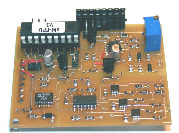
Math Coprocessor
The
Micromega uM-FPU_v3 integrated circuit is a very powerful math coprocessor
that is a computational subsystem all unto itself. The main Micro908
processor controls the math chip and transfers data to/from it via the
two-wire I2C bus. The math chip uses numerous 32-bit internal registers,
RAM, Flash and EEPROM memory to perform integer or floating point
computations (both common/low-level ones as well as complex scientific
functions) and a lookup table. The coprocessor in the math chip will allow
separate algorithmic computations to be performed in parallel with, or
instead of, the main Micro908 processor. Performance improvements may be
able to be achieved that will offset the extra transfer time for data across
the I2C bus. Experimentation and analysis is needed to verify the
performance impact/benefits of this math chip subsystem.
An
RS-232 level translator chip (MAX233) is also included on the REFL board in
order to provide connection of a dumb terminal for debug purposes with the
math subsystem. This will be an invaluable tool during the development
phase. This RS-232 debugging capability will not be provided on production
boards – the MAX233 chip will merely be omitted.
PC
Board Layout
Special care was taken to orient the Bridge and measurement components very
close to the edge of the REFL board and right up against the RF output jack
of the instrument. The two pads carrying the output signal may be soldered
directly to the back of the BNC connector, thus offering the most ideal
short-length connection to the instrument output. (Aside: Probably need
to determine a better connection method to the BNC that will allow
plug-removal of the REFL board.)
Understanding the electrically-sensitive nature of the measurement
subsystem, special consideration was also given to the ground plane layout.
A single ground “feed point” is located near the center of the REFL board,
which connects to four separate ground plane areas: (1) DDS and ALC; (2)
Bridge, Log Amps, Video Amps; (3) ADC; and (4) math.
Power Supplies
Two
TO92-packaged 3-terminal regulators provide 5V power for the REFL
components. One voltage regulator powers the ALC, log amps and video amp
circuits. The other voltage regulator powers the ADC and math subsystem.
The overall current draw of the REFL card with the DDS-60 plugged in is
approximately 270 ma.