-
Parts Inventory -- Make
sure you have all parts shown in the various items picture
above. Note that you might not have purchased some of
the options.
-
PCB Preparation -- Using
a fine-blade hack saw (or equiv), cut out the "X" areas in
each corner of the pcb to allow it to fit into the
enclosure. Be careful to cut "on the inside" of the
lines for the corner between J7and J2 so you don't
accidently cut the nearby trace on the bottom-side.
-
Attach BNC Connectors --
It may be necessary to file away a small recess on the edge
of the pcb to allow the BNCs to sit flush. (The
connectors have a small "lip" that otherwise gets in the way
of the connector sitting flush. It will be obvious when you
put the connector in place at first.) While holding
the BNC flat, solder the signal lead of the connector to its
pad on the pcb. This will tend to keep the connector
in position while you solder its shell to the board.
Now, using a
large-wattage soldering iron, attach the mounting tabs of
each BNC
connector, ensuring each is oriented as straight
(perpendicular to the board edge) as possible, and flat on
the pcb. Lots of heat is necessary to ensure good
connection of the all-metal connectors to the ground plane.
-
Attach Remaining
Connectors -- J1 (power), J5 (keyboard), J6 (serial),
J12 (2x20 display connector), and J8 (28-pin IC socket for
U1). Note that J5 may have a metal shell, which fits
into available holes.
-
Attach Power On/Off Switch --
S1 must be mounted straight (perpendicular to board edge and
flat against it.
-
Attach the 5V and 3.3V
"voltage regulator" components (caps too) -- 5V VR1 ("462NL53B"),
3.3V VR2 ("ZLDO17-33"), C8, C9, C10, C11, C12 and C13.
Note that the "negative" side of the electrolytic tin can
are indicated with a black stripe. Be sure you have
the orientation/polarity correct, and especially for C13,
which is oriented differently from the others.
[NOTE: We previously indicated that the large tab
on the VR2 package shouldn't be soldered down to the pad ...
It's really okay to do this, and you should for best
heatsinking!]
-
Test Board Voltages --
Apply power to the 2.1mm coaxial power connector J1 and
press the S1 switch "in" to turn the board on. Measure
12V, 5V and 3.3V at the respective marked test point (pads)
near each regulator. Do not proceed until you ensure
that you have the specified voltages on the test pads.
-
Attach Q2 and VR4 --
These little SOT-23 packages look alike. The package
ID for Q2 is "1P", and the package ID for VR4 is "RKA".
-
Attach U2, U3 and U4 Integrated
Circuits -- Carefully noting the pin 1 location for each
IC, insert and solder U2 and U3 (larger 20-pin DIP ICs), U4
(AD8307, the 8-pin SOIC). NOTE: The "U4"
location is actually labeled "U7" on the pc board.
(Oops!) Also, DO NOT yet insert U1 (the pre-programmed
28-pin dsPIC controller) into its socket.
-
Attach Q1 "2N7000" --
This TO92 package with its 3 leads on a "cardboard strip" is
a MOSFET transistor. Be sure to handle with anti-static care, form the leads to fit into
the offset pad locations, oriented with the flat side of the
transistor as indicated on the silkscreen.
-
Attach 5V Regulator VR3 -- Form the
leads to fit into the offset pad locations, oriented with
the flat side of the VR as indicated on the silkscreen.
-
Attach DDS Connector J4 --
Bend the pins on the 8-pin SIP receptacle at 90-deg
right at the body of the connector. Mount on the
bottom side of the pcb at the J4 position. Ensure that
the connector is at its max height by soldering the pins
just as they have entered the pcb pads. (That is, the
pins should not extend up past the top of the board.
Ensure that the resulting flat body of the connector is
parallel to the board and that the pins are at 90-deg to the
board.
-
Attach All Remaining Parts --
Be careful to note polarity/orientation of the small SMT
parts.
-
Note 1: The polarity of the speaker SPKR in upper-left
corner of the pcb. (+ sign in indicated on bottom of
part.)
-
Note 2: The 10uF SMT
capacitor C23 located near U4 is non-polarized, so it
doesn't matter which way you attach it.
-
Note 3: C5 is
supplied as a surface mount device (SMD) chip capacitor,
yet the board layout/silkscreen is for a larger
electrolytic capacitor. (Oops.) The SMD cap is
correct, so solder either end to one of the pads, and
use a short wire to connect the other end of the cap to
the other pad.)
-
Construct and attach L1 --
L1 is intended to be user-constructed. Wrap 1 turn of spare
hook-up wire around a Ľ” drill bit and attach as shown in
the website pics.
-
Attach Programming Connector
ICD1 -- Mount this 2x3 pinheader on the bottom side
of the pcb.
-
Attach 4 PCB Mounting
Standoffs -- Using the parts from the Enclosure Hardware
bag, attach the four aluminum standoffs on the bottom side
of the pcb, using the short 2x56 (smaller thread) screws.
-
Attach 2 Display Mounting
Standoffs -- Using the two, shorter 4-40 threaded
aluminum standoffs to the top of the pcb next to J2 and J3
BNCs.
-
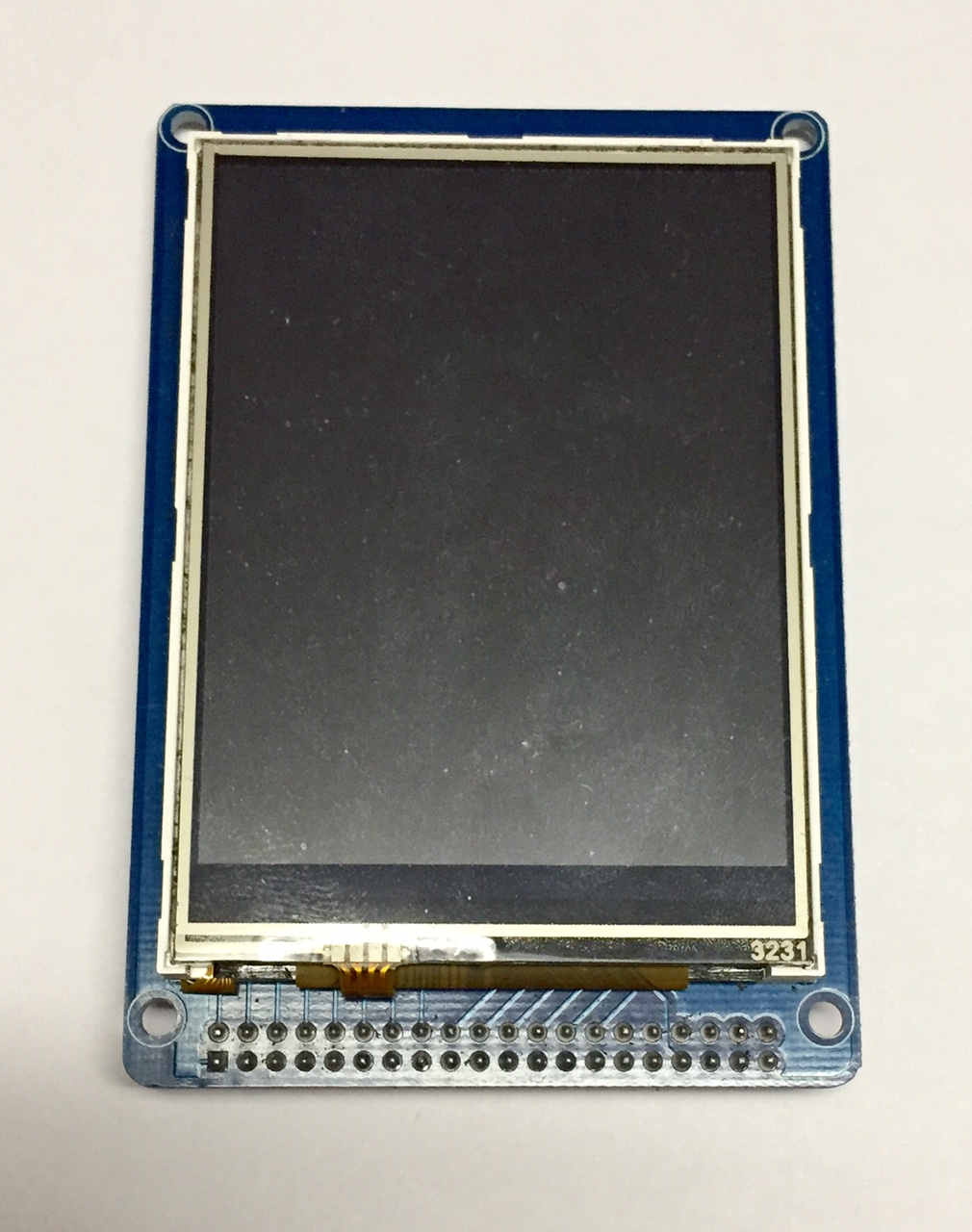
Attach U6 to Bottom of QVGA
Display -- Noting orientation of pin 1 on U6 (256 Kbit
EEPROM), attach to the IC1 position on the bottom of the
QVGA Display.
-
Plug the DDS-60 Card into J4
-- on the bottom of the board. Ensure proper
orientation of pin 1 on the DDS card. All assembled
DDS-60 cards purchased are tested before shipping.
1. Check
DC Levels ... Before
installing the dsPIC microcontroller and display module,
make one final check of the DC power levels.
2. Install
U1 and Display ... Install
the pre-programmed dsPIC processor U1 and the QVGA display module, making sure the display
connector is properly lined up with the connector on the PCBA. Do not install the MSNA assembly in its enclosure
until completing all the steps in this guide. You will need
access to components on the back of the main PCBA for
calibration.
3. Power
On! ... Leave
the SD card out, the keyboard unplugged, and then turn power
on.
4. Splash
Screen is Displayed ... After
a pause of up to five seconds, you should see the splash
screen showing the firmware revision level. (If you hold
your finger on the screen while the splash screen is
displayed, the splash screen will be displayed until you
raise your finger.)
5. Beep
Beep ... The
splash screen will be displayed for about 3 seconds and then
the Terminal mode screen will be displayed (top line for
keyboard input, blue area for output received from the
serial interface). You should also hear "GO" BEEPed in
Morse code ("--.
---").
6. So
Far So Good ... If
you got this far, there’s a good chance that everything is
working.
7. Plug
in Keyboard ... Turn
power off, plug in the keyboard, and turn power on again.
8. Keyboard
LEDs Flash ... You
should observe the same power up sequence as before except
this time you will see the LEDs on the keyboard flash twice,
the first time when power if first turned on and the second
time when the splash screen is finished and the MSNA resets
and initializes the keyboard. You should also hear a BEEP
at the time of the second LED flash.
9. Type
and See Text ... At
this point, characters typed on the keyboard should appear
on the input line. Pressing Enter on the keyboard
will send the text out the serial interface (3.5m stereo
jack) and clear the input line. Pressing and releasing the
Insert key will toggle the INS/OVR indicator in the
upper right corner of the display. Pressing Home
will clear any text on the input line.
10. Make
Loop-Back Connector ..
Make a
loop-back connector for the serial port that connects RxD to
TxD and connect it to the serial port. Now when you press
Enter on the keyboard, any text on the input line
will be sent out the TxD line and received back on the RxD
line and displayed in the blue output area of the display.
Pressing Alt-Home will clear any text in the output
area.
11. Scroll
Lock is Important ...
Press and
release the Scroll Lock key on the keyboard and
observe the Scroll Lock LED turning on. This indicates
successful two-way communication with the keyboard. (The
Caps Lock and the Num Lock keys and the
associated LEDs should also be working.)
12.
See
Command Mode Menu ... When the
Scroll Lock LED first comes on, the Command mode menu will
be displayed.
13.
F1 to
Display Data Entry Screen ... While in
Command mode, press F1 to display the data entry
screen. You will probably see garbage on the right side of
the display since this may be the first time the EEPROM has
been used. Use the UP ARROW and DOWN ARROW
keys to step through the data entry lines pressing Home
for each line to clear out the garbage. Then press Page
Down to select the second page and repeat the process to
clear these lines.
14.
Save All Changes ...
by pressing
Enter.
15.
Clear Data Fields for F1 ...
Press and
release Scroll Lock and press F1 again and
make sure the garbage is gone and all data entry fields are
blank. If they are not blank, there may be a problem with
the EEPROM on the display module. (Refer to Assembly step 16
above.) Double check the EEPROM placement and look for
solder bridges.
16.
Clear Data Fields for F2-F7 (optional) ...If you
like, repeat steps 11 through 15 for the function keys F2
through F7 and Alt-F1 through Alt-F7.
17.
Set
Baud Rate ... Select
Command mode (press and release Scroll Lock) again
and Select B (Serial Interface bps) to display the BAUD RATE
menu. Select 7 (38400 bps, the default) and press Enter
to save your selection to EEPROM.
18.
Insert
SD Card ... Insert a
properly formatted SD card (1GB or less, FAT16) in the SD
card receptacle on the display module. (NOTE: The SD
card supplied in the MNSA Kit is already formatted as
needed.)
19.
Switch
to DOS Mode ... Select
Command mode (press and release Scroll Lock) and
press the Escape key to switch to DOS mode.
20.
See
Data Files ... You will
see the DOS DIR command display showing the contents of the
first sector in the root directory on the SD card. Note
that if you inserted the SD card with power on, you may get
an error the first time you try to go into DOS mode. In
this case you will get a BEEP and the MSNA will remain in
Terminal mode. If this happens, make sure the SD card is
inserted properly and repeat the step 19.
21.
See
DOS Commands ... Press
Ctrl-M to display a list of the available DOS
commands. Even if you have not recorded any files on the SD
card, you can use the DUMP command to look at the data in
the Master Boot Sector, the FAT tables, and the ROOT
directory. If you have recorded text files on the SD card,
you can view their contents with the TYPE command. Be sure
to try the PENn command (n can be 1, 2, 3, or 6; any other
value is the same as 6).
22.
ESC and HOME Keys ...
Note that
after a DOS command has been executed, pressing Escape
will return to the DIR display and the MSNA will be ready to
accept another DOS command. Pressing the Home key
will clear any text on the input line. Pressing Escape
again will exit DOS mode and return to Terminal mode
23.
Calibrate the DDS Output Level and RF Power Meter ... Now you
have all the basic functions working so let's move on to
calibrate the RF Power Meter and the DDS output level. This
is best done by following Tutorial M1 that can be downloaded
from
http://midnightdesignsolutions.com/sna/documentation.html
24.
Calibrate the DDS ... After the
power levels have been calibrated, follow Tutorial 0 to
calibrate the DDS reference frequency.
25.
Mounting the PCB Assembly (PCBA) in the Enclosure ...
Now that
everything is working, you can mount the MSNA in its
enclosure by carefully angling the PCBA into the milled
enclosure. It may help to push in the S1 power switch
so it doesn't stick out quite as much, thus giving you a
little more room. Use the four remaining 2-56 screws (7/16")
to attach the PCBA through the four holes on the bottom side
of the enclosure. Some "compliance" was designed into
the mounting arrangement to allow you to slightly adjust the
position of the PCBA. Start by loosening the four pcb
mounting screws on the top of the board, then loosely screw
in the four longer screws on the bottom of the enclosure.
Align the PCB so all connectors and switches protruding from
the sides of the enclosure are centered within their cutout
areas, then carefully tighten down the eight screws that
hold everything together.
26.
Attaching the Front Panel Overlay ...
Apply strips of double-sticky tape around the backside
perimeter of the laminated Overlay. (Scotch brand
"Scrapbooking Tape" p/n 34-8700-9324-1 is perfect, but any
double-sided tape, rubber cement or glue works well too.)
With the enclosure lid screwed in place, carefully place the
Overlay on the front panel, ensuring that the four holes in
the corners are aligned over the four black screws that
mount the lid to the enclosure body. Firmly press down
on the Overlay (where the tape/glue is beneath) to ensure a
sufficient adherence to the plastic lid.
27.
Calibrating the Touch Screen ... Once you
have mounted the MSNA in its enclosure and verified
everything is still working, let's calibrate the touch
screen.
a. The
calibration function is started by touching the touch screen
when power is first turned on.
b. When
you see "TAP EACH CROSS" displayed, stop touching the screen
and the first cross will be displayed.
c. Touch
the center of the cross with a stylus. This is best done by
touching the screen and dragging the stylus to the center of
the cross and then raise the stylus. The MSNA records the
last point touched before raising the stylus.
d. After
the each cross has been touched, another cross will be
displayed. Touch each in sequence until all nine crosses
have been displayed and touched.
e. After
the last cross have been touched, the display will change to
a simple Etch-A-Sketch screen with two buttons at the
bottom. Use your stylus to draw on the screen and see how
close the drawn line follows the point of your stylus.
f. If
you are satisfied with the touch screen calibration, touch
the EXIT button and the MSNA will save the calibration data
in EEPROM and start normal operation.
g. If
you are not satisfied with the touch screen calibration,
touch the REDO button and the touch screen calibration
sequence will restart.
28.
Using
the MNSA with the PHSNA ... If you
plan to use your MSNA with a PHSNA system, do the following:
a. Connect
the serial interface as shown in the guide documents.
b. Power
up the UNO and if the PHSNA firmware has not been loaded in
the UNO, load it now.
c. Turn
on the MSNA and wait for the Terminal mode display.
d. Reset
the UNO and you should see the PHSNA startup information and
the main menu on the MSNA display. If you see garbage
characters, recheck your baud rates.
e. If,
instead of the Menu you see several lines of “CELL,GET,L2”
just wait. This line will be repeated about 30 times and
then the menu will be displayed. This means the PHSNA
firmware was in PLX mode when last turned off and that
information is kept in its EEPROM which determines the PHSNA
firmware startup mode. If this happens, you can use the
Options & Calibrations (‘*’ menu selection) to change the
default startup mode to NORMAL.
f. Key
‘0’ (zero) and Enter and the PHSNA main menu
should be displayed again indicating you have two-way
communication between the PHSNA firmware and the MSNA.


.JPG)